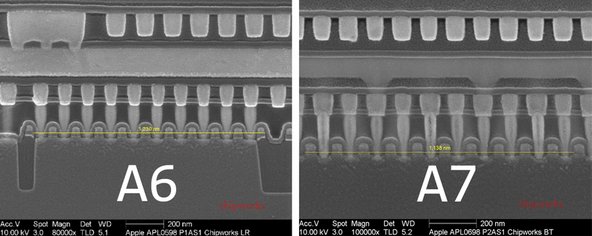
Last week, while we were disassembling the iPhone 5s into pieces, Chipworks was able to confirm that the manufacturer of Apple’s A7 processor was indeed Samsung. Not being content with their discovery, they delved into the A7 some more — this time by bringing out the big guns, in the form of an electron microscope. Below are a couple of images they shot:

Even we have issues figuring out what the heck we’re looking at in the image above, so we feel a bit of explanation is in order— and the M7, iSight camera, and other components came along for the ride. We present to you the Apple A7 Teardown.
Some fun tidbits regarding the A7’s cross-section:
- Every little hump (through which you see that yellow line) is a transistor. By measuring the total distance between ten of these transistors, we can estimate a chip’s manufacturing process — essentially how tightly the manufacturer can pack in all that processing power.
- Turns out that the A7’s “gate pitch” — the distance between each transistor — is 114 nm, compared to the A6’s 123 nm. Big whoop, you say?
- Those 9 nm are a big deal. It turns out that the A7 is made with the same 28 nm process as the eight-core Samsung Exynos 5410, the current flagship CPU for Samsung’s own Galaxy line.
- So what does that translate to? Applying some mathematrickery, this seemingly small change equates to having the same computing power, but in 77% of the original area. And given that the A7 processor is even larger in area than the A6, that means even more processing power to lead a healthy, smartphone-laden lifestyle.
We have tons more analysis of the A7, the M7, and supporting players in our teardown.


0 opmerkingen